


2021
July 5, 2021
MINEBEA MITSUMI Inc.
Notice regarding Establishment of New Semiconductor Design and Development Bases
MinebeaMitsumi Inc. (MinebeaMitsumi) hereby announces that we newly establish semiconductor design and development bases in Ota city, Gunma and Gifu city, Gifu from August 1.
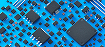
Analogue semiconductors are one of the "Eight Spears" (the company's strategy to identify our core business) and MinebeaMitsumi has promoted "INTEGRATION" activities to generate synergies between analogue semiconductors and other businesses such as motors.
On June 30, we announced a plan to acquire an 8-inch analogue semiconductor fabrication plant and MEMS business from OMRON Corporation. This time, in addition to the purpose of further strengthening the development capacity of analog semiconductor products, we establish new design and development bases for the purpose of strengthening the development of intelligent motor driver ICs that combine logic/CPU control technology and analog technology (which is our most important development products in the future for enhancing the line-up of our in-house motor driver ICs). We will hire approximately 60 semiconductor technology development members in Gunma and Gifu prefectures and this makes that we will have five semiconductor design and development bases in Japan including the Atsugi, Chitose, and Takatsuka bases. We aim to strengthen our semiconductor technology teams and further improve efficiency and performance of our driver IC development, mainly for in-house small and precision motors.
With the establishment of new bases, we will further promote "INTEGRATION" activities, and focus on providing close support to the market and customers and developing optimal products.
Outline of Gunma Office
| Name | Semiconductor Development Center Gunma Office |
|---|---|
| Location | Grandy Ota Building, 1053, Iida-cho, Ota city, Gunma (scheduled) |
| Starting date | August 1, 2021 |
| Main business | Design and development of analog semiconductors and mixed-signal semiconductors (with CPU core) centered on motor driver ICs |
Outline of Gifu Office
| Name | Semiconductor Development Center Gifu Office |
|---|---|
| Location | Nohhi Building, 2-20 Hashimoto-cho, Gifu city, Gifu (scheduled) |
| Starting date | August 1, 2021 |
| Main business | Design and development of mixed-signal semiconductors (with CPU core) centered on motor driver ICs |
* Mixed-signal semiconductor …
Analogue and digital mixed semiconductor equipped with analog circuits, large-scale digital circuits, CPU core etc.
| Media Inquiries | MinebeaMitsumi Inc. Corporate Communications and Investor Relations Office Phone: +81-(0)3-6758-6703 Fax: +81-(0)3-6758-6718 E-mail: koffice@minebeamitsumi.com |
|---|
Product information, contact and other context are subject to change without prior notice.

